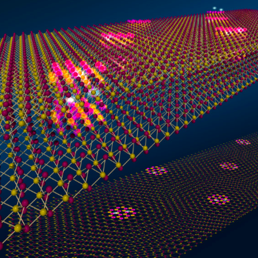
In early 2023, smartphones equipped with a metalens-enabled time-of-flight (ToF) sensor hit the market, the first commercially available metasurface technology to be used in consumer devices. The development came as a result of a partnership between Metalenz and semiconductor giant STMicroelectronics.
Unlike traditional moulded and curved lenses, metalens optics are completely planar, and are now being manufactured on silicon wafers alongside electronics in ST’s semiconductor front-end fabs for the first time. The meta-optics collect more light, provide multiple functions in a single layer, and enable new forms of sensing in smartphones and other devices, while taking up less space. Metalenz’s flat-lens technology replaces certain existing optics in ST’s FlightSense ToF modules, which serve applications such as smartphones, drones, robots, and vehicles. In these, ST has sold more than 1.7 billion units to date.
ST’s VL53L8CX sensor integrates a new generation VCSEL and two advanced meta-surface lenses. In the smartphone camera (the make of which has not yet been disclosed) the metalens sensor will aid the camera’s autofocus in taking more accurate distance measurements at high speeds, which enhances low-light imaging.
Lessons learned from metalens commercialisation
The commercial availability followed more than a decade of foundational research, according to Metalenz. Electro Optics spoke with Rob Devlin, the company’s co-founder and CEO, about bringing the technology to market.
What challenges did you have to overcome to carry your technology from the research stage to commercial product?
One of the things that normally is a big challenge for taking something from the lab and getting it out into the market is finding how to make it mass producible. You make a few in the lab; they perform in a certain way. You now need to make millions and millions of devices and get them all to perform in the same way and meet a customer spec. One of the major advantages with our metasurface optics is that they are made using existing semiconductor foundry processes, so fortunately volume and repeatability are not the major challenges. That’s one of the big benefits that has allowed us to scale so quickly.
The biggest challenge for our technology, and really any new technology, is convincing a customer to take that risk of adoption. It means you can’t just be a few per cent better on some metric. You must be displacing a true pain point for them. No one ever gets fired for improving the incumbent by 5% year over year, but if a company takes a risk on a new technology and it doesn’t work, that can be a big problem. For Metalenz, the biggest challenge was building up champions, showing that our technology has true real-world advantages – more than just on paper and prototypes.
What advances have made it possible to bring metalenses into the commercial realm?
Often the normal thing is to have some new manufacturing process come along and open possibilities. But in this case, we didn’t need a new manufacturing process to drive this. There were two main things; first, at the technology level, when metasurfaces were first demonstrated in Federico Capasso’s [Harvard] group, everyone saw the promise of the proof of concept, but the performance really was not there for them to be practical in real world devices.
So, the first thing was optimising the performance and making sure that the designs were mass producible. That was the basis of the demonstration that we had in 2016, where we showed the first high-quality images from metasurfaces. You could actually get really high-quality images because the performance had been boosted so much through optimisation simulation.
Second, on the application side, metasurfaces can simplify optical systems dramatically, but still need to work within a narrow bandwidth range. There weren’t any large consumer narrow-band imaging applications prior to around 2016, when the company was founded, but then you had the launch of facial recognition in phones – and, for the first time, 3D sensing as a narrow band imaging application became a mass consumer market. And it was a perfect fit for the technology because those 3D imaging systems are much more complicated than the typical 2D imaging system that we’re used to.
What advice do you have to start-ups trying to bring a new technology to market?
Know your audience and their pain points. First, take a very hard look at whatever you’re doing and make sure that you’re solving a deep pain point for the customer. Unless you have a substantial improvement or a complete displacement of a way of doing things that you know solve something for the customer, the likelihood of landing, finalising, getting designed in, and getting the design win is not very high because, at the end of the day, if you’re not offering a huge, distinct advantage then it’s difficult to displace incumbent technology.
What technical and business factors do you think were instrumental in forming a partnership with STMicroelectronics?
The first thing was that metasurface optics had a natural product market fit in 3D sensing and STMicroelectronics is one of the leading 3D sensing module manufacturers, so they could immediately see the benefit that our optics could bring across their entire system. The second piece again comes back to the mass production process. We are using all solid-state, semiconductor materials. We’re making our lenses out of silicon, so when it came to putting our technology into consumer applications where all these materials and processes are already used, it ultimately led to quicker adoption.
What challenges exist for selling into the consumer market, and how do you address these?
I think in general with the consumer market, it’s hundreds of millions of devices that you’re going into, so you need to have the scale. Our business model as a fabless company leveraging existing semiconductor foundries gave us this scale potential from day one. Foundries can produce hundreds of billions of chips daily. Also, the metasurface is so simple in terms of process – a factor of 20-30 times simpler than the typical chips that they’re manufacturing. Using the semiconductor foundry to make our metasurface optics allows us to pass through the gates of scale, reliability, and repeatability most efficiently.
As a growing company with roots as a University spin-off, how does Metalenz achieve a balance between growing a business and continuing to research and innovate?
Getting a new technology into the market takes an element of laser focus, where you need to make sure you’re getting the right product market fit. As a growing company, we benefit from a few things; first and key is that Metalenz is a fabless semiconductor company. This allows us to devote our resources to design and new applications of metasurfaces. We don’t need a huge operation and can stay light on our feet without being distracted by running factories and foundries. This allows us to make sure we continue to keep an eye to future applications, new designs, new ways of using our optics. It allows us to follow through on getting the product out there in a market like we have. We can also continue innovating with new products, new applications, entirely new forms of sensing like we’re now doing with PolarEyes for example, bringing polarisation to consumer markets for the first time. Second, we benefit from a continued relationship with the Harvard lab and the Capasso group – the founding group of this field. As interesting new things are invented around metasurfaces from the group, we can leverage that and bring it into the company for the longer-horizon type of applications 5 to 10 years out.
How do you stay in tune with what the future needs of the markets you sell into?
The way that we stay in tune with the future needs of the markets that we’re selling into is by solving customer pain points today. Once you’ve done that and established that credibility, you are given a clearer view of road maps and where the market is headed. Making sure you get in in the first place takes a lot of footwork and effort and iterations. In addition, knowing your technology deeply and continuing to do business development and looking at all the possibilities as you gain new technical insights, you establish a feedback loop with the customer. Because you have that relationship, you can go to the customer and say: “Hey, I can do this really interesting thing – is there anything you find it useful for?” It’s a mutually beneficial relationship built on credibility and listening to the markets, and where they want to go.


