A new 3D printing method has been developed that can produce complex devices with multiple materials – including plastics, metals and semiconductors – with a single machine.
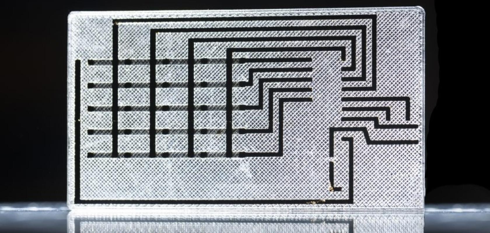
The technique, developed at the University of Missouri, has been used to manufacture multi-layered sensors, circuit boards and even textiles with electronic components.
By printing sensors embedded within different structures, sensors could be incorporated into a wider range of objects to monitor temperature and pressure, for example, or medical parameters. This could advance research monitoring the environment, or improve wearable devices that monitor blood pressure and other vital signs.
“This opens the possibility for entirely new markets,” said Jian ‘Javen’ Lin, an associate professor of mechanical and aerospace engineering. “It will have broad impacts on wearable sensors, customisable robots, medical devices and more.”
Printing circuit boards typically requires multiple steps
Currently, manufacturing a multi-layered structure – such as a printed circuit board – can be a cumbersome process that involves multiple steps and materials. These processes are costly, time consuming, and can generate waste that harms the environment.
Specifically, techniques fall short when it comes to how versatile the material can be and how precisely smaller components can be placed inside larger 3D structures.
Called ‘Freeform Multi-material Assembly Process’, the Missouri team’s machine has three different nozzles: one adds ink-like material; another uses a laser to carve shapes and materials; and the third adds additional functional materials to enhance the product's capabilities.
It starts by producing a basic structure with regular 3D printing filament, such as polycarbonate, a type of transparent thermoplastic. Then, it switches to the laser to convert some parts into a special material called laser-induced graphene, putting it exactly where it's needed. Finally, more materials are added to enhance the functional abilities of the final product.
The work is being funded by the National Science Foundation (NSF) Advanced Manufacturing programme, and the NSF I-Corps programme is providing funds to explore commercialisation.
“Currently, we believe it would be of interest to other researchers, but we believe it will ultimately benefit businesses," said Lin. "It will shorten fabrication time for device prototyping by allowing companies to make prototypes in house. This technology, available only at Mizzou, shows great promise for transforming the way products are fabricated and manufactured.”
The work was recently published in Nature Communications.
