A new approach for measuring photonic microchips with much higher precision, speed, and sensitivity has received funding from the Dutch Research Council (NWO).
The laser-based method, developed at Vrije University in Amsterdam, promises 100 times higher spectral resolution, 1,000 times higher sensitivity, and real-time operation.
Having already proved its working principle, the team now aims to expand the method’s operating bandwidth and explore new application areas.
We speak to project lead Imran Avci about the technology behind the method, and how her team works with photonics companies.
How does the PIC measurement method work?
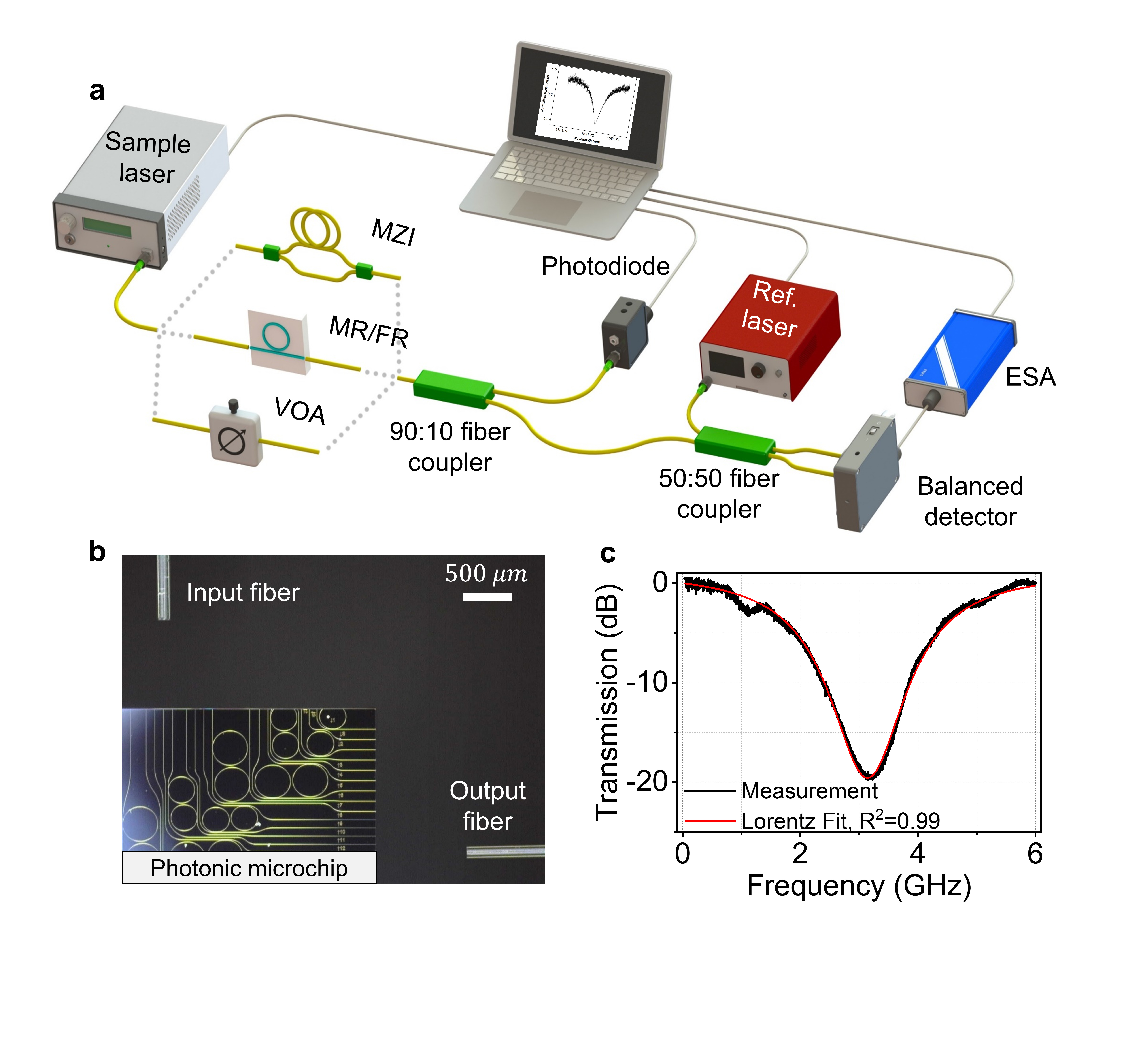
The setup of the measurement technique, called the ‘Sweeping optical frequency mixing method (SOHO)”, is shown in Figure 1a.
A sample laser (Emcore TTX1995 micro-ITLA) is coupled to the photonic microchip via a single-mode optical fibre after passing through a polarisation controller. The light coming out of the microchip is sent through a 90/10 splitter, and 90% of the light is sent to an amplified photodiode (Thorlabs, DET08CFC/M). This part of the setup is a commonly-used tunable laser-based characterisation setup (termed ‘standard method’), which we embedded into the SOHO setup to enable a direct comparison between the two methods.

Fig. 1. a (top): Schematic of the experimental setup of SOHO. b (bottom): The measurement configuration that was used to test the relaxed coupling requirements of SOHO (image: M. M. Dashtabi, et. al, Laser Photonics Rev 2024, 18, 2301396. https://doi.org/10.1002/lpor.202301396
The remaining 10% of the light is combined with the reference laser (Thorlabs, WDM8-C-23A-20nm) through a 50/50 coupler and is sent into a high-speed balanced detector (Thorlabs, BDX3BA). A polarisation controller was employed after the reference laser. When the frequency difference of the sample and the reference lasers are within the bandwidth of the photodetector, a beat frequency equal to the difference between the frequencies of the two lasers is detected on the balanced photodetector and measured with the electrical spectrum analyser (ESA, Signal Hound, BB60D).
The output signal has an intensity proportional to the product of the amplitudes of the two lasers. SOHO allows for measuring a spectral window width that is twice the electrical bandwidth without the need to scan the reference laser. Control of lasers, reading the ESA output, and data processing are done using a custom code written in C#.
The method enables the measurement of optical cavities or interferometers at a much higher accuracy and sensitivity in real time. Compared to the standard method, it has a 1,000 times higher sensitivity and a hundred times higher spectral resolution.
How will this method work within its target application?
The target application for now is the characterisation of photonic integrated circuits, in particular micro-ring resonators and interferometers, which are used in various applications ranging from quantum to optical biosensing.
The SOHO method can be used as a first check to measure the performance of photonic microchips, or as a readout method for certain applications such as biosensing.
One of the more significant benefits is that it eliminates the need for stringent alignment requirements between photonic microchips and optical fibres as shown in Fig. 1b. This is mainly important for optical biosensors as they need to be disposable.
What are the next steps towards commercialisation?
We want to increase the bandwidth of the system and also demonstrate a similar system at 800nm to expand its application range, and the NWO grant will help us achieve these goals. We will also make a business plan and form collaborations to tailor our final system design toward the needs of the users. We already filed a patent application for this idea, which will help us to secure some subsidies for the next step.
What off-the-shelf optical components do you wish existed that could help this project?
Lasers with better stability (no dithering) at near infrared wavelength ranges.
How do you work with optical/photonic companies currently, and how could this be improved?
I am collaborating with some of these companies or I buy my components from them. For grant applications, some of them provide support letters and support my projects in kind and in cash.
I had to build this network myself, which is usually very difficult for junior scientists. It would be useful if something could be done to make building connections easier.
I also think that companies should financially support scientific research more if they want to find a solution to their problems. Large companies are doing this but it is insufficient. We need to find a way to better support one another.
If you had a magic wand, what would you change to advance your research?
Access to cutting-edge fabrication tools would allow my team to push the boundaries of integrated optics, accelerating innovation and enabling us to tackle the most complex technical challenges without constraint.


