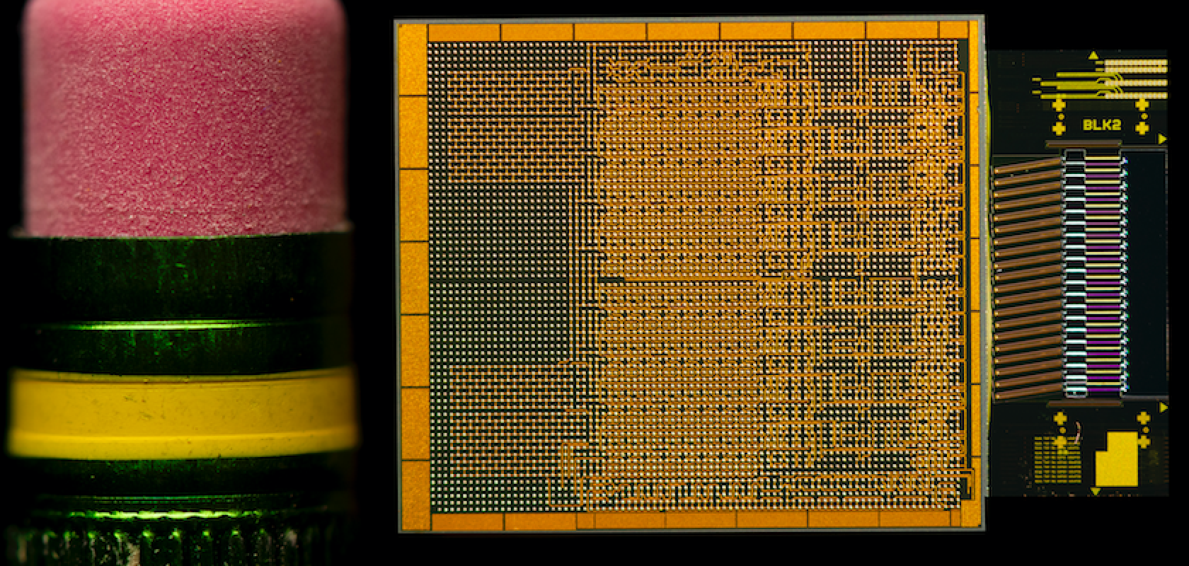
Intel’s Integrated Photonics Solutions (IPS) Group has demonstrated the ‘first-ever fully integrated optical compute interconnect (OCI) chiplet co-packaged with an Intel CPU and running live data’ at the Optical Fibre Communication Conference (OFC) 2024.
IPS says its technology is the industry’s most advanced OCI and represents a development in high-bandwidth interconnect, enabling co-packaged optical input/output (I/O) in emerging AI infrastructure for data centres and high performance computing (HPC) applications.
Enabling high-speed data transmission, the OCI chiplet is designed to support 64 channels of 32GBPs data transmission in each direction on up to 100m of fibre optics, potentially helping to address AI infrastructure’s growing demands for higher bandwidth, lower power consumption and longer reach.
Intel says the solution is remarkably energy efficient, consuming only 5 pico-Joules (pJ) per bit compared to pluggable optical transceiver modules at about 15 pJ/bit.
What are the specifications of the new chiplet?
To make such achievements possible, the fully Integrated OCI chiplet harnesses Intel’s silicon photonics technology and integrates a silicon photonics integrated circuit, which includes on-chip lasers and optical amplifiers.
This first OCI implementation supports up to four terabits per second bidirectional data transfer, compatible with peripheral component interconnect express Gen5. The live optical link demonstration showcases a transmitter and receiver connection between two CPU platforms over a single-mode fibre patch cord.
The CPUs generated and measured the optical bit error rate, and the demonstration showcased the optical spectrum with eight wavelengths at 200GHz spacing on a single fibre.
The OCI chiplet demonstrated at OFC was co-packaged with an Intel CPU, but can also be integrated with next-generation CPUs, GPUs, IPUs and other system-on-chips.
What benefits does the chipper offer?
Such features are particularly useful given AI’s demand for exponential growth in I/O bandwidth and longer reach to support larger processing unit clusters and architectures with more efficient resource utilisation, including xPU disaggregation and memory pooling.
This is because the co-packaged xPU optical I/O solution can support higher bandwidths with improved power efficiency, low latency and longer reach – exactly what AI/ML infrastructure scaling requires. Intel says the jump in technology from electrical I/O with optical I/O in CPUs and GPUs to transfer data is like going from using horse-drawn carriages to distribute goods to using cars and trucks that can deliver much larger quantities of goods over much longer distances.
Thomas Liljeberg, senior director, Product Management and Strategy, Integrated Photonics Solutions Group, said: “The ever-increasing movement of data from server to server is straining the capabilities of today’s data center infrastructure, and current solutions are rapidly approaching the practical limits of electrical I/O performance. However, Intel’s groundbreaking achievement empowers customers to seamlessly integrate co-packaged silicon photonics interconnect solutions into next-generation compute systems. Our OCI chiplet boosts bandwidth, reduces power consumption and increases reach, enabling ML workload acceleration that promises to revolutionise high-performance AI infrastructure.”
Additionally, the chiplet will be able to enable future scalability of CPU/GPU cluster connectivity and novel compute architectures, including coherent memory, according to IPS.
What’s next for Intel?
Next generation, 200G/lane PICs to support emerging 800Gbps and 1.6Tbps applications are under development. Intel says it is also implementing a new silicon photonics fab process node with state-of-the-art device performance, higher density, better coupling and vastly improved economics.
While the current OCI chiplet is a prototype, Intel is already working with select customers to co-package OCI with their SoCs as an optical I/O solution.
Lead image: Intel


