Dutch firm Morphotonics has raised more than $10 million to ramp up its roll-to-plate (R2P) production technology for display optics.
Based on lithography, Morphotonics’ machines can add lenses, prisms, and other complex structures onto substrates - such as glass or foils - to produce ‘any optics, for any display, at any size’.
This enables the creation of next-generation products, the company says, including intuitive 3D displays, outdoor-readable smartphones, and immersive AR smart glasses, at a lower cost.
The new funds will expand the company's focus beyond displays to target products in the semiconductor packaging and biotechnology sectors.
Large substrates for trillions of integrated lenses
Unlike traditional lithography, Morphotonics’ large-area R2P nanoimprint technology allows the processing of ‘large’ substrates of up to 1.1 x 1.3 metres, with the integration of trillions of lenses now possible.
“Micron and nano structures of all different shapes and types (from 500 micron down to 50 nm) can be replicated on such large surfaces using our R2P technology and equipment,” said Erhan Ercan, Head of Global Business Development.
Examples of complex display optics include lenticular lenses (used in 3D displays), binary/blazed/slanted gratings as waveguides inside AR glasses, and anti-reflection/anti-glare surfaces for mobile device screens, Ercan told Electro Optics.
Complex optics for additional applications include light trapping structures, solar panels, microneedles for biosensor devices, hydrophobic structures for antifouling for boats, among others.
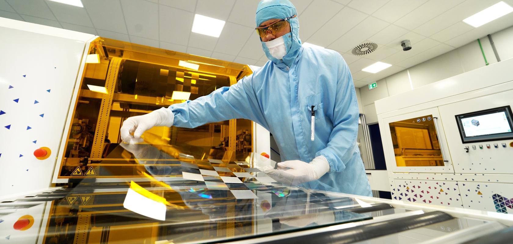
During R2P nanoimprinting, the substrate is first primed and a resin coating is deposited. A flexible stamp, which contains the inverted version of the desired structure, is laminated onto the substrate. The resin fills this stamp and is cured with UV light, before being removed, leaving the desired structure on the substrate.
The main advantages include design freedom, scalable manufacturing, and cost, Ercan said.
“It allows designers freedom of choice in selecting more complicated micron and nano textures that otherwise would not be manufacturable,” he said. “And, due to the use of larger substrates, per unit production cost of such micron/nano textures can be significantly cheaper, making them commercially feasible to use.”
Moving into semiconductor packaging and biotechnology
Currently, the company has more than 20 equipment installations worldwide for customers, ranging from “large consumer electronics brands to big contract manufacturers and everything in between, from start-ups to academic institutions,” said Ercan.
3D display company Leia is one customer using the technology for mass production; their LumePad 3D displays feature an optical layer produced on Morphotonics’ machines.
A portion of the new funding will be used to finalise the development and commercialisation of fully automated versions of the company’s large-area nanoimprint machines, and the first customer unit is currently being built with delivery expected in 2025.
Additionally, it aims to develop equipment that can replicate structures with even greater precision where the lenses are located (for instance, adding lenses with precise position accuracy on display pixels), while maintaining large substrate sizes.
“With these two advancements, we will expand our focus beyond displays and target products in the semiconductor packaging and biotechnology sectors,” Ercan said.
Scalable manufacturing regardless of the underlying display tech
R2P technology can also be used despite the varying underlying manufacturing method or technologies used within displays (for example OLED, LCD, microLED).
This is because, regardless of whether OLEDs, LCDs or microLEDs are used, all displays require a ‘light management layer’ either in front of or behind the display panel to optimise light performance.
“The role of this layer can vary. It might be used to collimate or trap light, improving efficiency and reducing power consumption,” Ercan explained.
Alternatively, it may serve specific functions, such as guiding, magnifying, or reshaping the photons produced by the display panel.
“Hence, our large-area nanoimprint technology can create such light management layers regardless of the display technology used,” said Ercan.
The company’s series B financing round included new investors 3M and Brabant Development Agency (BOM) and existing investor Innovation Industries.
