Researchers have discovered how an ultrathin material can circularly polarise light, setting up a promising approach of manipulating light for applications in optoelectronic devices.
The research represents an important insight into ultrathin structures known as two-dimensional (2D) materials, which can enable smaller and more functional optical instruments.
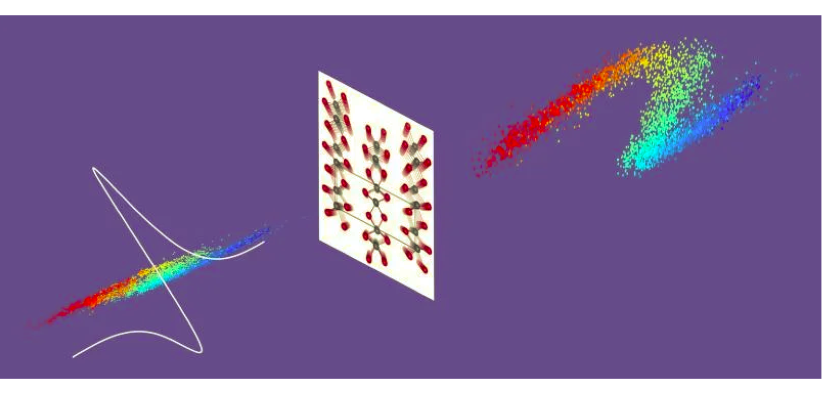
The new behaviour was discovered at the US Department of Energy’s National Accelerator Laboratory at Stanford University, using an instrument for ultrafast electron diffraction (MeV-UED), a world-leading tools for ultrafast science.
Terahertz offers new optical design oportunities
Terahertz radiation enables novel ways of both characterising and controlling the properties of materials. Figuring out a way to harness that light could advance the development of future optoelectronic devices.
Using the MeV-UED, the Stanford team found that when oriented in a specific direction and subjected to linear terahertz radiation, an ultrathin film of tungsten ditelluride – which has desirable properties for polarising light used in optical devices – circularly polarises the incoming light.
Whereas the MeV-UED is normally used to visualise the motion of atoms by measuring how they scatter electrons after hitting a sample with an electron beam, this new work used the femtosecond electron pulses to visualise the electric and magnetic fields of the incoming terahertz pulses, which caused the electrons to wiggle back and forth.
In the research, circular polarisation was indicated by images of the electrons that showed a circular pattern rather than a straight line.
The ultrathin material was a mere 50 nanometres thick, which is “1,000 to 10,000 times thinner than what we typically need to induce this type of response,” said Stanford professor Aaron Lindenberg, who led the research.
Two-dimensional materials to advance optoelectronic devices
Researchers are excited about using these ultrathin materials, known as two-dimensional (2D) materials, to make optoelectronic devices smaller and capable of more functions. They envision creating devices from layers of 2D structures, like stacking Legos, Lindenberg said. Each 2D structure would be composed of a different material, precisely aligned to generate a specific type of optical response.
These different structures and functionalities can be combined into compact devices that could find potential applications – for example, in medical imaging or other types of optoelectronic devices.
“This work represents another element in our toolbox for manipulating terahertz light fields, which in turn could allow for new ways to control materials and devices in interesting ways,” said Lindenberg.
The research was recently published in Nano Letters.
