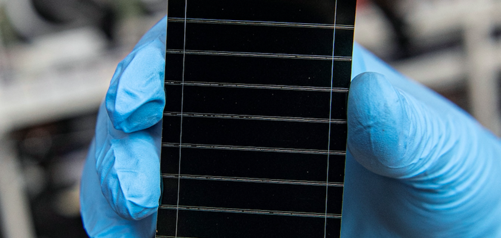
A team of researchers has developed a technique to precisely engineer layered hybrid perovskites (LHPs) at the atomic level, enabling controlled conversion of electrical charge into light.
The research, published in Matter, and conducted by researchers from North Carolina State University (NC State), with contributions from Brookhaven National Laboratory, is hoped to open up new possibilities for designing materials with highly efficient optoelectronic properties. Specifically, hybrid LHPs could contribute to the development of next-generation printed LEDs, lasers, and other photonic technologies.
LHPs, which are composed of thin layers of perovskite semiconductor material separated by organic spacers, are valued for their ability to efficiently convert electrical charge into light. The researchers even noted that LHPs based on iodide have been researched for photovoltaic applications due to their superior stability thanks to their oriented growth. While these characteristics make them promising candidates for use in optoelectronic applications, their power conversion efficiency has trailed 3D perovskites which have reached 26%.
Until now, there has been limited understanding of how to manipulate their atomic structure to improve performance, despite the interest in LHPs.
Controlling energy flows within materials
The researchers’ findings revolve around the structure of quantum wells – thin sheets of semiconductor material sandwiched between organic layers – which are crucial for controlling how LHPs conduct energy. According to the research, the size distribution of these quantum wells plays a key role in how energy flows within the material.
Professor Aram Amassian of NC State, who co-authored the study, explained: “We knew quantum wells were forming in LHPs – they’re the layers. The team discovered that controlling the distribution of quantum wells – specifically ensuring a smooth transition between wells of different thickness –improves energy efficiency within the material.”
Professor Kenan Gundogdu, another co-author on the paper, elaborated: “A quantum well that is two atoms thick has higher energy than a quantum well that is five atoms thick. And in order to get energy to flow efficiently, you want to have quantum wells that are three and four atoms thick between the quantum wells that are two and five atoms thick.”
However, the researchers encountered a discrepancy between two common measurement techniques. X-ray diffraction data, a method used to investigate the structural properties of materials at the atomic or molecular level, often suggested quantum wells of a uniform thickness. On the other hand, optical spectroscopy, which measured the spectrum of light being absorbed, emitted, or scattered, detected a range of thicknesses. This anomaly led the researchers to investigate further, ultimately uncovering the role of nanoplatelets.
Understanding nanoplatelets and how they inform quantum wells
The researchers found that these nanoplatelets act as templates for the quantum wells, dictating their thickness. As the nanoplatelets grow over time, the quantum wells beneath them follow suit, eventually becoming three-dimensional crystals. Amassian went on to explain: “Nanoplatelets are individual sheets of the perovskite material that form on the surface of the solution we use to create LHPs.”
Crucially, the team also discovered a way to halt this growth, allowing them to control the size and distribution of quantum wells. By controlling the size and arrangement of the quantum wells, the researchers were able to successfully create energy cascades – which means the material is highly efficient and fast at funnelling charges and energy for the purposes of laser and LED applications.
Amassian added: “To control the growth of nanoplatelets we monitored their ripening using optical spectroscopy and used the antisolvent drip method to stop them from growing further. The antisolvent method is known to dry the precursor feeding the nanoplatelets by wicking away the solvent. By timing the antisolvent drip with the ripening of the nanoplatelets we achieved size control of quantum wells.”
He continued: “We optically pumped LHPs fabricated with controlled growth of quantum wells using the above described antisolvent drip method and we observed consistently low threshold of amplified emission which are desirable for lasers. The values obtained are low for LHPs. What was important in the context of LHPs was achieving these values reproducibly. Another important observation was the demonstration of excellent photostability and amplified emission of these LHP samples in ambient air.”
Looking beyond LHPs, the researchers also tested whether this method could be applied to other perovskite materials, such as those used in solar cells. It was subsequently confirmed that the technique could also improve the structure and efficiency of materials used in photovoltaic technologies.


