Researchers from the University of Twente in the Netherlands have discovered that photons confined inside 3D cavity superlattices can take on extremely unique shapes, much more so than electronic orbitals in solid state.
The work pertains to electrons in atomic crystals and photons in photonic crystals, which could advance numerous applications, especially in designing novel photonic devices.
Controlling photon orbitals
In atoms, minuscule elementary particles called electrons occupy regions around the nucleus in shapes called orbitals. These orbitals give the probability of finding an electron in a particular region of space. Quantum mechanics determines the shape and energy of these orbitals. Similarly to electrons, researchers describe the region of space where a photon is most likely found with orbitals too.
Researchers at the University of Twente studied these photonic orbitals and discovered that with careful design of specific materials, they can create and control these orbitals with a great variety of shapes and symmetries. These results have potential applications in advanced optical technologies and quantum computing.
“In textbook chemistry, the electrons always orbit around the tiny atomic core at the centre of the orbital – so, an electron orbital shape cannot deviate much from a perfect sphere,” said Marek Kozoň, first author of a paper published in Physical Review B. “With photons, the orbitals can have whatever wild shape you design by combining different optical materials in designed spatial arrangements.”
Ease of design could advance optical technologies
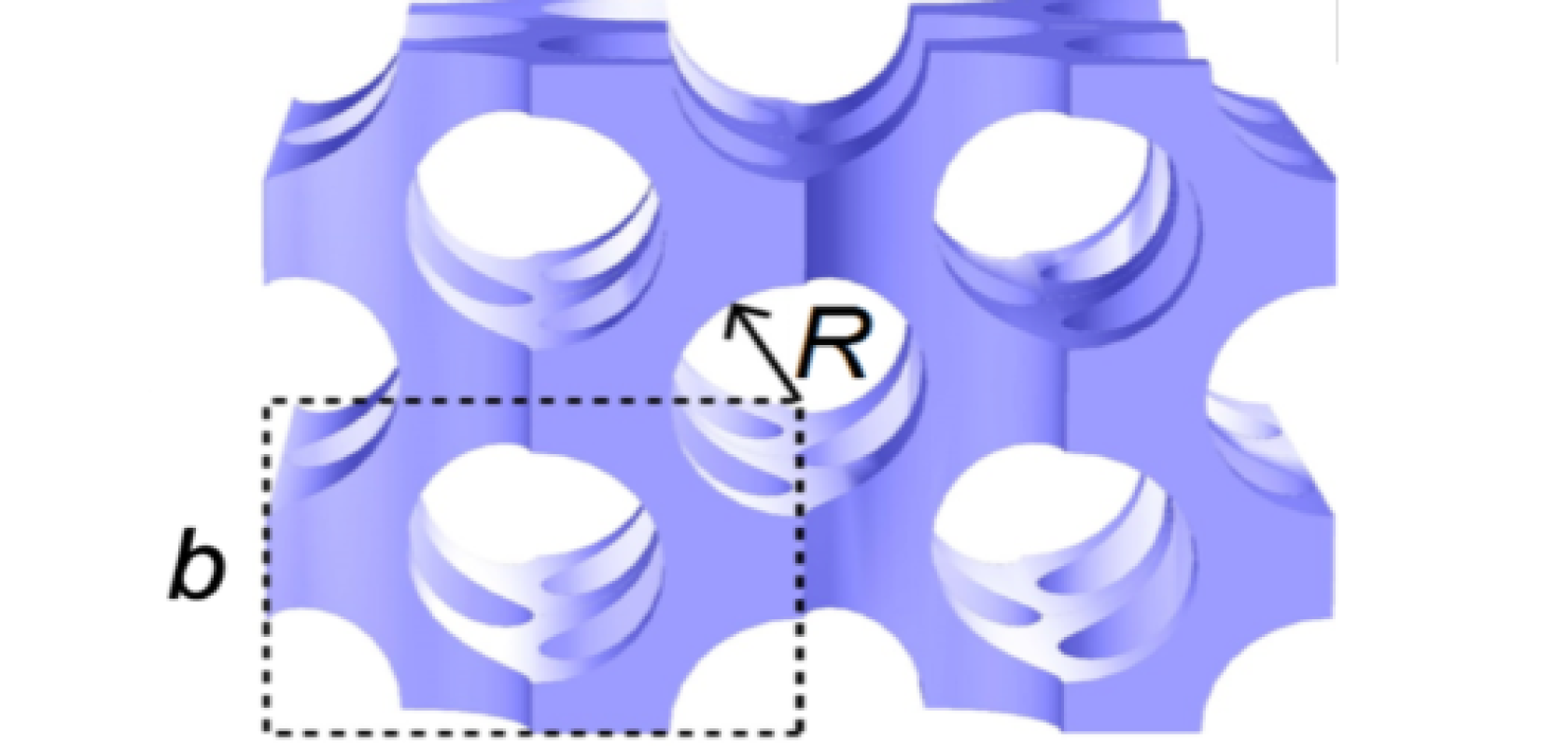
The researchers conducted a computational study to understand how photons behave when they are confined in a specific 3D nanostructure consisting of tiny pores (a photonic crystal). These cavities are intentionally designed to have defects, creating a superstructure that isolates the photonic states from the surrounding environment.
“Given the rich toolbox in nanotechnology, it is much easier to design nifty nanostructures with novel photonic orbitals than it is to modify atoms to realise novel electronic orbitals and chemistry,” said Physicists Vos and Lagendijk.
Photonic orbitals are important for developing advanced optical technologies, such as efficient lighting, quantum computing, and sensitive photonic sensors.
The researchers also studied how these nanostructures enhance the local density of optical states, which is important for applications in cavity quantum electrodynamics. They found that structures with smaller defects reveal greater enhancement than those with larger defects. This makes them more suitable for integrating quantum dots and creating networks of single photons.
