Researchers from the Institute of Photonic Sciences (ICFO) in Spain, and US-based technology firm Corning have developed a new method for fabricating anti-reflective surfaces using a lithography-free process.
The method uses thermally dewetted silver as an etching mask to create nanohole structures on glass surfaces, significantly reducing light reflection. This provides new possible solutions to the development of optoelectronic devices that require high transmission and durability.
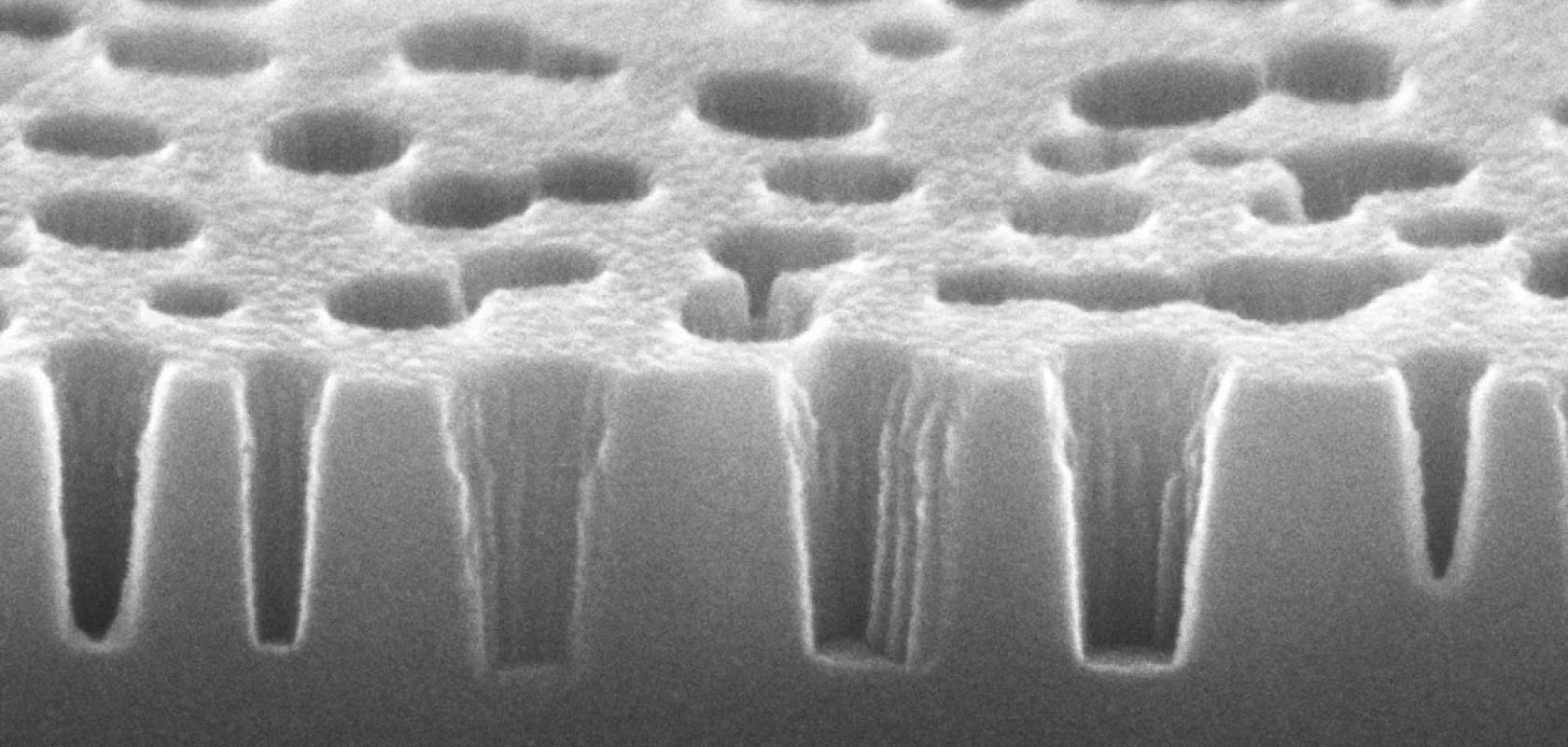
Nanostructures enhance efficiency of optical devices, but their fabrication is complex
Anti-reflective (AR) surfaces are valued for their ability to minimise unwanted reflections, enhancing the efficiency of various optical devices such as laser optics, camera lenses, eyeglasses, touchscreen displays, and solar harvesting systems.
Several alternative strategies to that of the traditional multilayer anti-reflective coating procedure have been developed to increase the performance and versatility of optical devices. Using bio-inspired nano-scale structures, such as nanopillars or nanoholes, directly onto a substrate surface enables the manipulation of light paths and reduces the reflection across a broad spectrum and wide range of angles.
However, the fabrication of these nano-structured surfaces with the desired properties is rather complex, often involving multi-step lithography methods, limiting their widespread adoption due to cost and scalability constraints.
Lithography-free method provides a simple and cost effective fabrication option
The ICFO/Corning method achieves nanostructured AR surfaces using a simple, cost-effective method that avoids complex lithography. Through the use of thermally dewetted thin silver films as etching masks, subwavelength nanohole structures can be generated on the glass surfaces.
The fabrication process involves three main steps. Initially, silver nanoparticles are obtained by quickly thermally annealing an ultra-thin silver film onto a glass substrate. These particles then serve as a base for a secondary etching mask, created by depositing a thin nickel layer over the silver nanoparticles and performing selective chemical wet etching.
Finally, this mask is used in a dry etching process to carve nanoholes of varying depths into the glass surface.
"Nanoholes are tiny, irregularly arranged cavities on a surface that significantly reduce light reflection by smoothly transitioning the refractive index from air to substrate," explained Iliyan Karadzhov, an early-stage researcher at ICFO in the NANO-GLASS project. "They were chosen for their superior mechanical durability compared to other nanostructures like nanopillars and their ability to provide excellent AR properties with minimal light scattering," adds the first author of the study.
The final arrangement and depth of these nanoholes are determined by the initial thickness of the silver film and the duration of the dry etch process. The team fabricated several samples with varying initial masks and hole depths, testing their performance by measuring both transmittance and reflectance in the visible and near-infrared ranges. The newly developed AR surfaces exhibited a broadband omnidirectional response that achieves transmittance levels exceeding 99% in both the visible and near-infrared ranges, as well as maintaining high transmittance even at steep angles of incidence (up to 60°).
The samples also demonstrated mechanical robustness and durability in abrasion tests. "One challenge was ensuring that the nanohole structures remained intact during abrasion tests while maintaining high optical performance," said Karl Koch, a researcher at Corning Incorporated. "This was overcome by optimising the nanoholes' geometry and the fabrication process to balance the mechanical and optical properties.
Another challenge was scaling the fabrication method for large-area applications, Koch added, which was addressed by leveraging scalable techniques such as thermal dewetting.
The research was recently described in the journal ACS Applied Materials and Interfaces.
